
UCSB is using three approaches:
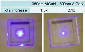
- The first uses an AlGaN layer for vertical mode control and confinement, which is relatively easy to fabricate and provides moderate performance of up to 75%. However, this relies on the quality of the AlGaN layer. Increasing the aluminum composition provides better optical confinement, but thicker layers can result in cracking, which results in a lower IQE.
- The second approach uses substrate lift-off and layer thinning. Extraction efficiency is a factor of cavity thickness and quantum well position, with the two factors presenting a tradeoff. Although this method presents challenges in fabrication, has metal absorption losses, and can result in damage during the fabrication process, UCSB is pursuing more tests because the performance has the potential to reach 90+%.
- The third approach is to use lateral epitaxial overgrowth (LEO). This method is also challenging to fabricate, but because of the thin active layer, it can be patterned before the active region is grown, which achieves vertical mode control. This results in no fabrication damage or material overgrowth, and provides intermediate performance of about 80+%. Researchers at UCSB are encouraged by the coalescence achieved using this method, as it is very important at the nanoscale dimension.
UCSB anticipates that advances being sought in large area patterning and fabrication of devices will pave the pathway to manufacturable processes. The research team has concluded that microcavity and photonic crystal LEDs both require vertical confinement of light and low loss metal mirrors. Since confinement of the AlGaN layer is a major growth challenge, the team is also trying other materials such as Aluminum Nitride. Thinned LLO layers by selective etching have proven promising, because the process is scalable to larger sizes. However, this requires better metal contacts to provide the high performance being sought. Finally, the LEO approach puts a major challenge on 2D thin LEO coalescence and growth, but it may provide the ultimate solution if these obstacles are overcome. UCSB will continue to apply vertical mode engineering and photonic crystal technology to extract more light from LEDs.
Return to Research Highlights