
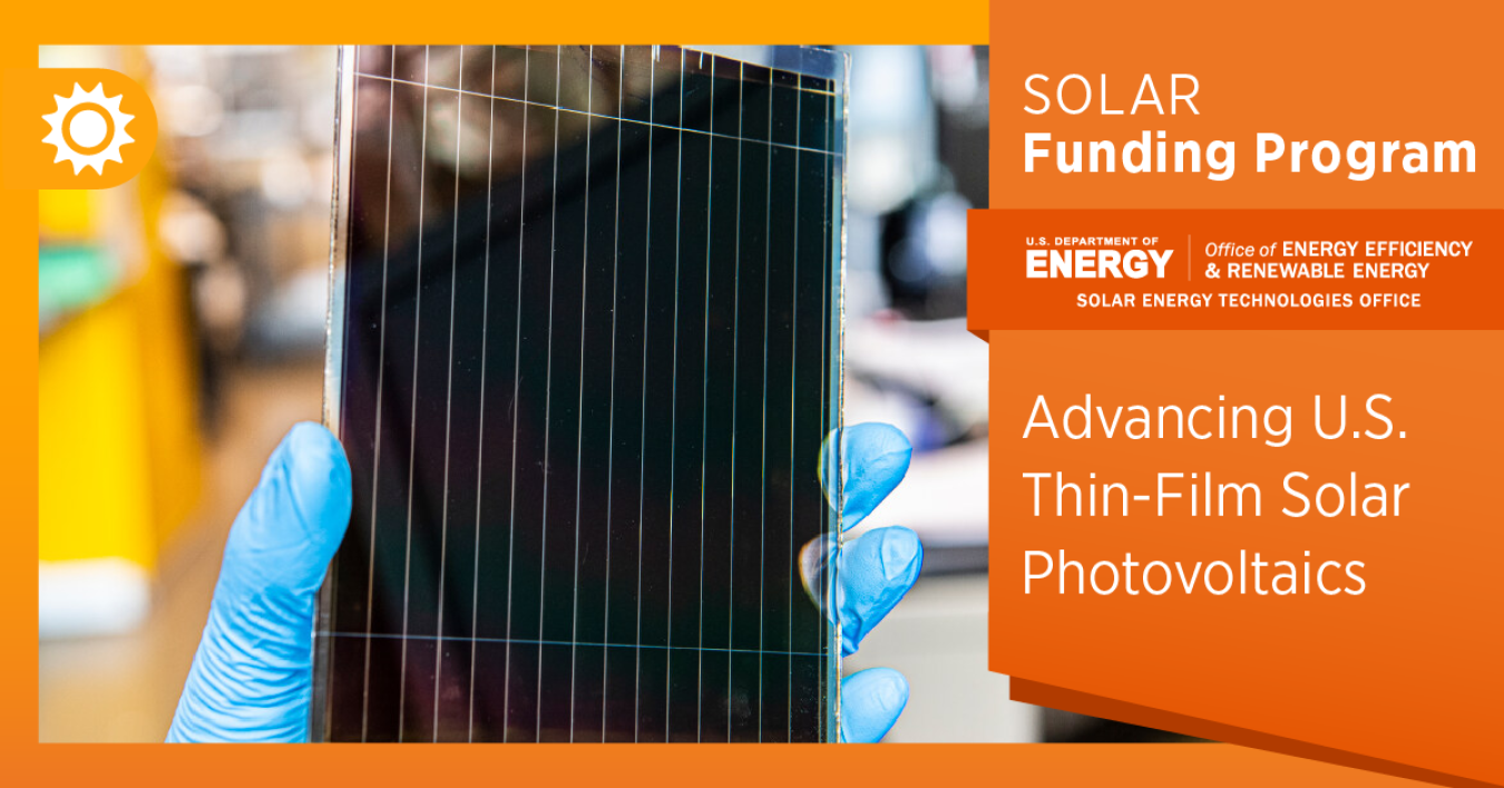
The Advancing U.S. Thin-Film Solar Photovoltaics funding program awards $44 million for research, development, and demonstration projects on two major thin-film photovoltaic (PV) technologies. Projects will help enable domestic manufacturing of affordable solar hardware, increase the portion of solar hardware value kept in the U.S. economy, and promote American leadership of thin-film PV technologies.
The U.S. Department of Energy (DOE) Solar Energy Technologies Office (SETO) announced the funding opportunity on September 12, 2023 and announced selections on May 16, 2024.
Approach
Projects will de-risk tandem thin-film technologies that include perovskite materials. Projects will also support innovation in cadmium telluride (CdTe) production by improving efficiency and reducing costs, making CdTe systems more affordable and improving competitiveness of the domestic CdTe industry. Advancement of thin-film technologies presents an opportunity to strengthen the domestic solar supply chain and reduce reliance on foreign imports.
Objective
This funding program supports an equitable transition to a decarbonized electricity system by 2035 and facilitates secure, robust, and reliable integration of solar electricity into the nation’s energy grid.
Selectees
– Award and cost share amounts are rounded and subject to change pending negotiations –
Topic 1: Promoting Research & Development toward Industrial Manufacturing of Early-Stage Perovskite Tandem Photovoltaics (PRIMES Perovskite Tandem PV)
Cubic PV
Project Name: Scaling Perovskite-Silicon Tandems Toward Reliable Commercial Product
Location: Bedford, MA
DOE Award Amount: $6 million
Awardee Cost Share: $1.5 million
Principal Investigator: Adam Lorenz
Project Description: This project aims to design perovskite-silicon tandem PV modules that can be fabricated using robust manufacturing methods and remain durable after exposure to heat and light. The team will use a four-terminal device configuration, which allows for optimization of the perovskite device layer without changing the silicon layer. By closely monitoring the devices throughout the perovskite layer fabrication process, the team can quickly and specifically identify the effects of any changes and ensure the final process will create reproducible, durable devices.
First Solar
Project Name: High‐Performance Tandem Modules Based on Wide‐bandgap FAPbI3 Perovskites and Narrow‐bandgap CI(G)S Bottom Cells
Location: Perrysburg, OH
DOE Award Amount: $6 million
Awardee Cost Share: $1.5 million
Principal Investigator: Le Chen
Project Description: This project aims to design tandem perovskite and copper indium gallium diselenide (CIGS) PV modules with 27% efficiency that can be easily manufactured. The team will maximize the efficiency of the perovskite layer and optimize the properties of the CIGS layer to best complement the perovskite layer. They will also scale up these devices from minimodule size and perform durability tests to ensure these devices are stable over time and practical to manufacture.
Swift Solar
Project Name: PIPPIN: Perovskite-Silicon Tandem Solar Cells from Prototype to Production
Location: San Carlos, CA
DOE Award Amount: $7 million
Awardee Cost Share: $1.8 million
Principal Investigator: Rohit Prasanna
Project Description: This project is developing durable, high-efficiency, perovskite-silicon tandem PV modules where the perovskite layer is fabricated using vapor deposition, a promising method for high-volume manufacturing. The team will incorporate measurements throughout the manufacturing process to improve process control and reproducibility while testing the durability of their modules to ensure they can reliably operate for decades in the field.
Tandem PV
Project Name: STACKED: Stability and Characterization of Hole-Transporting Layers Key to Enabling Outdoor Durability
Location: San Jose, CA
DOE Award Amount: $4.7 million
Awardee Cost Share: $2 million
Principal Investigator: Colin Bailie
Project Description: Ultraviolet (UV) light from the sun can cause significant damage to perovskite PV devices, but current simulated outdoor durability testing does not adequately account for its effects. This project aims to engineer UV hardness into critical layers in perovskite PV devices that also increase durability under high temperatures. The team will perform enhanced durability testing on tandem perovskite-silicon devices with these new layers to ensure they are stable and retain their high efficiency in outdoor conditions.
Topic 2: Improving the Market Potential of Advanced Cadmium Telluride Photovoltaics (IMPACdTe PV)
5N Plus
Project Name: Upstream Extraction of Tellurium from Copper Concentrates
Location: Montreal, Quebec
DOE Award Amount: $1.6 million
Awardee Cost Share: $400,000
Principal Investigator: Frederic Belanger
Project Description: A major barrier to increasing CdTe PV module production is the availability of tellurium (Te), an element necessary to manufacture CdTe PV cells that currently has a very limited supply. Most Te is obtained from ore extracted for copper mining, but the current processing methods only extract 3-4% of the available Te in this ore, with the rest being discarded during other processing steps. This project aims to increase Te supply by developing an innovative extraction method that will recover more Te from the copper ore earlier in the process. This method will also extract toxic elements like antimony and arsenic, making the copper mining process more environmentally friendly.
BrightSpot Automation
Project Name: Lifecycle Reliability Testing of CdTe Solar Panels
Location: Boulder, CO
DOE Award Amount: $1.6 million
Awardee Cost Share: $400,000
Principal Investigator: Andrew Gabor
Project Description: This project aims to develop an imaging method to detect damage to in CdTe PV modules in the field. The team will design, build, and test a non-invasive, high-throughput imaging tool using photoluminescence, which works by shining light onto the PV panels and measuring light that shines back in response. The team will develop artificial intelligence software to correlate specific types of defects with changes seen in the photoluminescence data from the imaging tool. Automated defect detection will reduce investment risks, lower financing and insurance costs, improve system performance, and inform panel end-of-life decisions.
First Solar
Project Name: High-Density Interconnect Technology for CdTe PV Modules
Location: Perrysburg, OH
DOE Award Amount: $15 million
Awardee Cost Share: $27 million
Principal Investigator: Rui Shao
Project Description: This project aims to increase CdTe PV module efficiency using an innovative three-dimensional design for electrical contacts in the PV cell. While this design has shown promise in smaller-scale experiments, this project will demonstrate that this design for electrical contacts can be scaled up for use in high-volume manufacturing to create more efficient, reliable, cost-effective CdTe modules.
Tau Sciences
Project Name: MANTIS: From Multiscale Analysis to Next Generation Thin Film Module Inspection Systems
Location: Redwood City, CA
DOE Award Amount: $2.1 million
Awardee Cost Share: $500,000
Principal Investigator: Gregory Horner
Project Description: This project is developing a new non-contact inspection technology to detect defects in CdTe PV modules, enabling site owners to detect problems, quantify the potential impact, and respond accordingly. Information gained through defect detection methods can also increase investor confidence in CdTe PV plants. The team will develop two different imaging techniques that measure how PV panels respond to electrical current and infrared light, then correlate these responses to specific defects.
Learn more about the Solar Energy Technologies Office’s manufacturing and competitiveness research, funding programs, and open funding opportunities.