
Photo
Caption
The one-electron transistor. Transistors are building blocks for all microelectronics.
Credit
Zyvex Labs
Photo

Caption
Lab-Embedded Entrepreneurship Program participant Yu Kambe is commercializing a Quantum Dot ink to enable the manufacturing of energy-efficient, tricolor micro-displays for virtual and augmented-reality devices.
Credit
NanoPattern Technologies, Inc., Chain Reaction Innovations, ANL
Photo
Caption
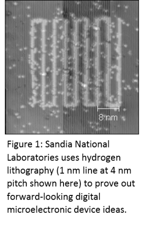
Sandia National Laboratories (SNL) uses hydrogen lithography to create a one-nanometer line to validate digital, microelectronic device ideas. The sharp right angles depicted here literally enable a knife-edge potential well to trap electrons, enabling a tenfold improvement in the efficiency of electronic transistors for “edge computing.”
Credit
SNL
Photo

Caption
New manufacturing methods allow atoms to be deposited one layer at a time. In this image, a single layer of atoms covers the “trenches” shown in silicon, a material commonly used in conventional electronics components.
Credit
RMD Inc.
Photo

Caption
Nanoscale-device measurements depicted here, combined with machine-learning and artificial intelligence at the SLAC National Accelerator Laboratory, will enable researchers to develop integrated, microelectronic systems that are 10 times more energy efficient than today’s best systems. SLAC’s breakthrough technology will allow circuits to be manufactured in 3D, using techniques (e.g., atomic-layer deposition, AI-guided non-equilibrium flash annealing process) to make next-generation computing platforms (e.g., with unprecedented ferroelectric HfO2-ZrO2 thin film on-chip capacitors) that overcome Moore's law and the energy-efficiency limitations of today’s computer architecture.
Credit
SLAC
Photo
Caption
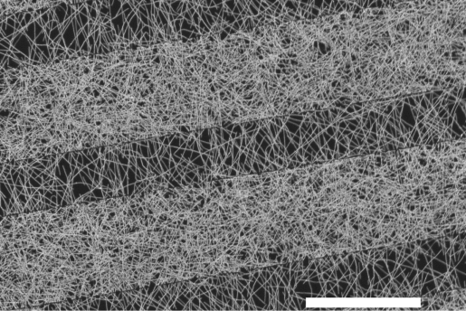
The unique properties of carbon nanotubes (dark stripes) make them applicable for highly energy-efficient semiconductor technology and electronic devices.
Credit
Carbon Technology, Inc.
Photo

Caption
By selectively precipitating metallic-carbon nanotubes and leaving semiconducting-carbon nanotubes dispersed in solution, Lab-Embedded Entrepreneurship Program participant William Fitzhugh is developing an approach for low-cost supply chains for manufacturing next-generation nanoelectronics.
Credit
American Nanotechnologies, Innovation Crossroads, ORNL
Photo
Caption
Lab-Embedded Entrepreneurship Program participant Chad Husko of Iris Light Technologies in the Chain Reaction Innovations program at Argonne National Laboratory is using nanomaterials to make smaller, more efficient lasers for advanced photonics. Researchers are working to link photonics to electronics to improve speed and efficiency.
Credit
Iris Light Technologies, Chain Reaction Innovations, ANL
Photo
Caption
The one-electron transistor. Transistors are building blocks for all microelectronics.
Credit
Zyvex Labs
The one-electron transistor. Transistors are building blocks for all microelectronics.
Zyvex Labs
February 14, 2025